Table of Contents
Logic Analyzer
Years ago I found the sump.org FPGA Based Logic Analyzer project and decided that I have to build a logic analyzer (LA). At this time I already owned the same Xilinx FPGA board he used so there was not much work left for me.
Still until I got the time (and some pressure needing a LA) building it it took about three years. All the components I collected in the meantime. I used some nice HP logic analyzer flying leads but they are not worth the time for this project (Below more about this).
I'm really proud about the case for my LA. My first try was a nice aluminum box (from a hdd enclosure) but it was not possible to fit the PCB inside it. So the project was laying around a while and sometimes I tried something also laying around if it could fit as a case.
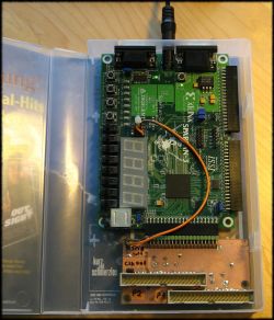
So I found out that this LA perfectly fits into a VHS cassette case. What a nice coincident! This makes this part extremely cheap and as you have seen on the pictures, your LA will look way cooler than any of your other measurement equipment. I went to a thrift shop to find VHS cases with nice covers or skins 
You need the VHS cases which are transparent, else you don't see the LED display (Which is extremely helpful for debugging).
Level Shifter
It was clear for me that when I build a LA then it needs a useful wide input voltage range. On the project page there is the 2.5 - 5.0V Input Stage Using TI SN74ALVTH16244 add-on which does this. There are several reasons why it was not possible to use there PCB for my LA.
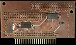
I made an own version of this input stage, it is more compact, well designed for home made PCBs and providing a connector layout to make it easier to make proper probes for it. It measures 89 x 45 mm.
This is the schematic of the input stage levelshifter-schematic.pdf it only has a different connector layout compared to the original one.
Here is a picture of the finished level shifter input stage (bottom side):
Most vias are easily accessible so you don't need a plated PCB. Only the vias for ground under the IC's are not accessible, you have to solder them as flat as possible.
I used gEDA for this project, all files you need (layout artwork, partlist, gEDA files) are in this archive: levelshifter.tar.gz
Probes
I have to talk a bit about probes for this LA input stage.
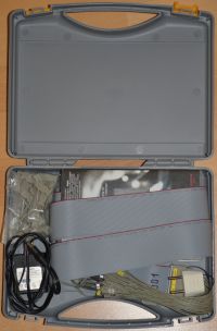
I worked with HP/Agilent logic analyzers and really like there accessories to connect your target. Because of that I liked to use old HP flying leads adapters for my LA.
The connector layout is really good, they use for every signal line a ground wire. The ground wire is parallel to the signal wire and follows it to the probe pin. There it is left open. This is needed to achieve a good quality for high speed signals.
During testing of my level shifter and the LA I noticed some difference when using the probes and testing with direct wires to GND or VCC. First here was no difference using the probes without the level shifter. The problem with the HP probes, for this specific LA, is that they also have a series resistor built in, directly behind the probe end. It's a 15k ohm resistor, this is a good thing for an LA, to limit the influence to the target. The input stage of a LA has to be build with this in mind. The simple level shifter input stage here and also the FPGA input pins are not build for this. Due to the level shifter IC's bus hold feature the outputs are stuck. The FPGA pins suffer from really bad signal quality due to the big impedance mismatch.
To easily build probes for this level shifter board use 40 pin ribbon cable with one connector on one side. On the other cable side you build your probe ends. Split the cable end into pairs of two wires. Split up to the length you think you need to have enough to connect your targets. To every wire pair solder a single pin socket for square pins (to the signal wire). Let the ground wire open. Use shrinking tube to hold the single pin socket with the ground wire together and to protect the solder joint. Add small numbers to the probe wires to identify them.
Links
Main project page, you should find all related information there including FAQ and user contributed help:
http://www.sump.org/projects/analyzer/
Project page for the PC client (old, don't use anymore):
http://sourceforge.net/projects/jlac/ Original
http://www.lxtreme.nl/ols/ Alternative PC client project
PC software:
http://sigrok.org/ Use sigrok and Pulseview. The sigrok project aims at creating a portable, cross-platform, Free/Libre/Open-Source signal analysis software suite that supports various device types (e.g. logic analyzers, oscilloscopes, and many more).
Really good user guide. You could ship the sump.org LA with this manual as a comercial product:
Oak Micros Logic Analyzer User Guide
Usefull Trigger output extension to the VHDL model:
Patch to make the Sump logic analzyer emit a rougly 600uS trigger output


Discussion
Warning: Undefined array key "id" in /home/brain4fr/public_html/brain4free.cyon.site/wiki/lib/plugins/discussion/action.php on line 834
Rich, 2010/06/09 04:00
Nice project. Forrest mims used the case for his haze meter in the may1997 Scientific american magazine Amateur Scientist. I have also found them a nice fit for projects.
http://web.archive.org/web/20020202030436/http://www.sciam.com/0597issue/0597amsci.html